Quick Schematic Guide to programming FPGA's using Intels Quartus II programming Suite.

Goals :-
- Quartus II (Web Version 15.0) install
- Schematic drawing and Custom Gate Modules
- Pin Allocations
- GPIO :- Button inputs and led (7 segment) outputs
- Compile and Up-loading to the De0 Nano
1. Quartus II (Intel's Web Version 15.0) install
The following walkthrough will be using the Quartus II Web version 15.0 software suite
During install just select the bare minimum for the FPGA Chip Set you are using to enable a "lighter" version.
In the case of the De0 Nano it just needs support for the Altera Cyclone IV FPGA chip.
On start up select the New Project Wizard.

Enter your project directory "Project_MRL"...project name as "Project_MRL" and lastly call the top entity file "Project_MRL_top".
Press "Finish" as other settings are not really necessary till chip programming time.

2. Schematic drawing
Some like writing reams of code..... and others like drawing code (I am the latter).
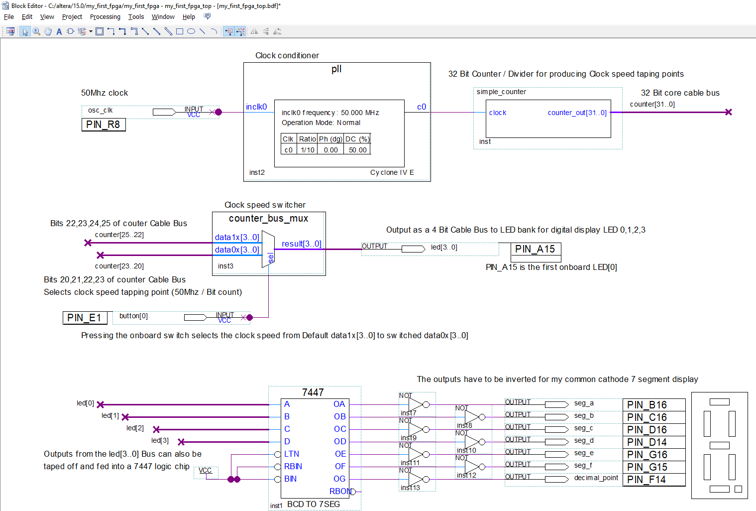
For this project we will need a clock .... and a divider to tame the system clock from 50Mhz down into the 1hz range.
Under "File - New" select "Block Diagram/Schematic File" .

A file window (drawing canvas) opens, good idea to save it ......"Save As ..Project_MRL_top.bdf".
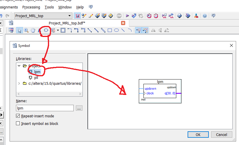
Now we need to create a schematic clock control (aka PLL phase Locked Loop)
Under "View - Utility Window - IP Catalog", type "ALTPLL" into the IP Catalog's search bar. and double click the found "ALTPLL" entry and name the file it opens "pll"
The ALTPLL schematic Wizard pops up , update the frequency, the de0 Nano clock runs at 50Mhz

Under the Inputs/Lock uncheck all entries (these are not required for this project) ,

Then simply "Finish" to create and save the Schematic files, good idea to check all the boxes.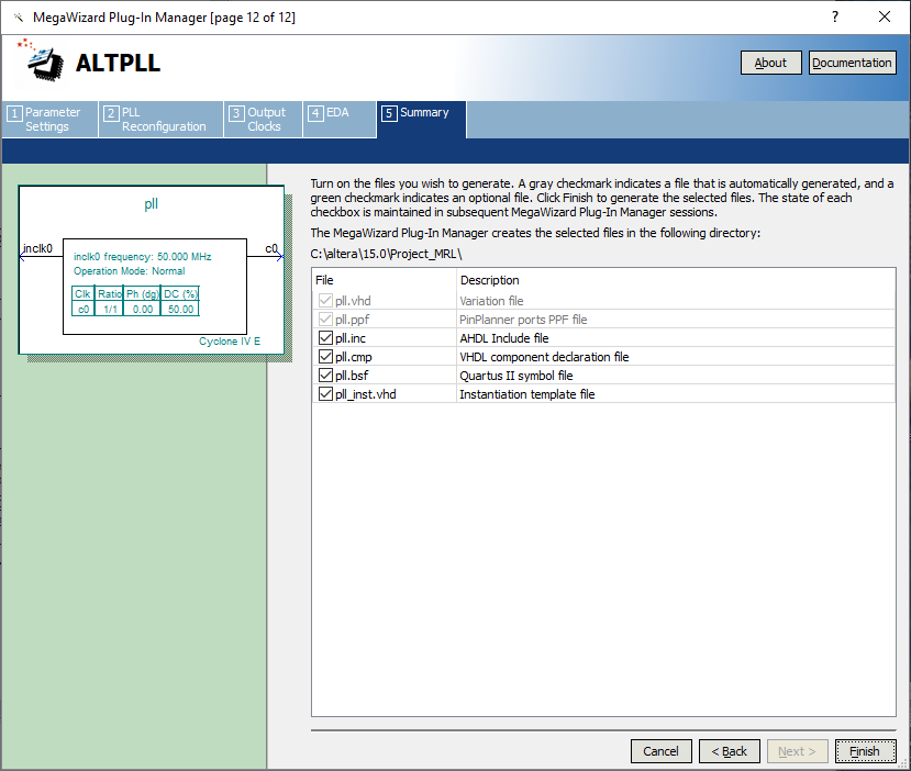
Now we have created it you can find it as a Logic entity
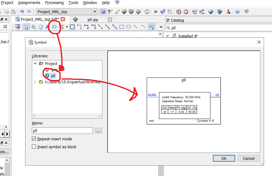
Ok it and Drop it onto your blank canvas.
Because the User clock operates at 50Mhz we need to tame it down a tad (to circa 1hz so we can see blinky led's etcetc).
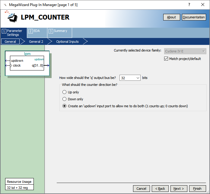
To do this we will add a LPM_COUNTER. library of parametrized module (LPM !!!)
Under "View - Utility Window - IP Catalog" type "LPM_COUNTER" into the IP Catalog's search bar. and double click the "LPM_COUNTER" and name the file "pll"
Our clock will be using a 32 bit counter , (if you divide 50Mhz by 26 bits you will get into the 1hz range).
As an extra control we will add an extra up and down counter pin.
"Finish" and name the file "lpm"
Now we have created it you can find it as a Logic entity
Ok it and Drop this onto the Canvas right of the PLL

Now some wiring ....
- Select the pin tool - (Input pin) (red) and drop it onto the inclk0 (this is the 50Mhz clock source). double click the input pin and rename it "osc_clk"
- Select Orthogonal Node Tool (green) and use it to connect a wire between "c0" of the pll to the "clock" input of the lpm.
- Select the Orthogonal Bus Tool (blue) and simply select the output pin and draw a short bus line out from it ..Right click it and with its properties - rename it to "counter[31..0]", this effectively converts it to multiway cable bus with 32 wires wrapped within.
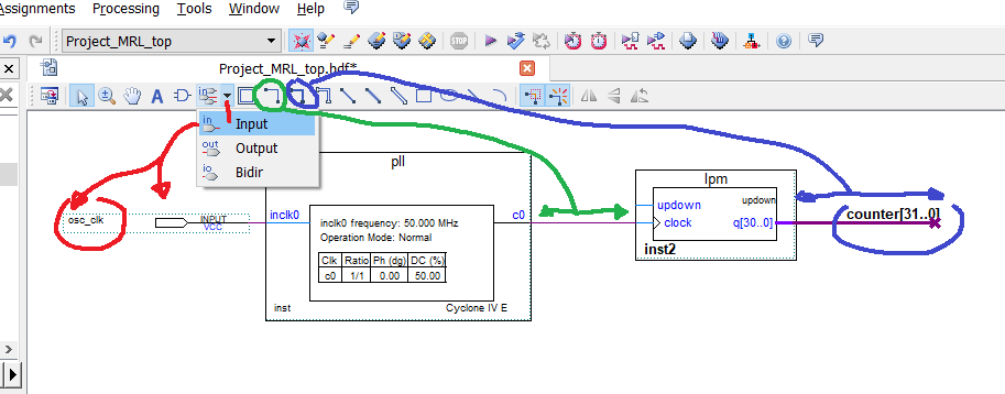
This sets up the clock and clock divider chain.
3.Pin Assignments
Next we have to set up Quartus to the Chip Set we are using ....
The De0 Nano uses EP4CE22F17C6N Cyclone iv
Under Assignments - Device ... scroll through the available devices and select EP4CE22F17C6 and Ok it.
This also sets up the compiler directives peculiar to the chip set.
Then Assignments - Pin Planner .... a neat interactive hieroglyphic Wire Bond Gui pops up .
At the moment we only need to link our clock osc_clk to PIN_R8 (50Mhz)....
Its a simple case of grabbing the osc_clk and literally dropping it onto PIN_R8 .
4. GPIO :- Button inputs and led (7 segment) outputs
The FPGA library holds a host of logic gates and best of all almost the whole TTL logic chip set.
We will choose a TTL 7447 BCD>7 SEG chip ... binary coded decimal (though this chip was pre HEX days so anything after nine is garbage).
Using the Gui Symbol Tool,search for the 7447 and drop onto canvas, also pick up and drop 7 NOT gates and a VCC supply line. draw the link lines with the Orthogonal Node Tool.
Using the Gui Pin Tool pick up 7 Output pins and rename them (double click) seg_a to seg_g (aka 7 segments) and also a Input pin and rename it KEY1 for the onboard tactile switch and connect it to the lpm's updown pin
Using the Orthogonal Bus Tool draw 4 bus lines into the 7447 A,B,C,D input pins and re_label them (right click properties) to counter[24] , counter[25], counter[26] and counter[27]
So you will end up with this wiring diagram :-

Note-worthy is the Output Bus of the lpm counter[31..0] , individual bits off this Bus can be gleamed out as single control wires.... referenced so ....counter[22] for the 22 bit. makes wiring really neat.
To tidy up and sync everything with the Pin assignments run the :- "Processing - Start - Start Analysis & Synthesis" process, this will clean up the labels and tidy up the Pin Planner.

Fire up the Pin Assignment Gui and drag and drop the seg_a ,b,c,d,e,f,g to the relevant output pins and also the tactile switch KEY1 to pin E1 which will be the up/down counter control.

That sets up all the pins..... time to compile and Upload to the FPGA chip
5. Compile and Up-loading to the De0 Nano
Using the tab "Processing - Start Compilation" starts up the compiler and this outputs a Project_MRL_top.sof file which you will find in the projects output_files folder.

Using Tab .... "Tool - Programmer" or the programmer icon, then "Add file" "Project_MRL_top.sof"

and "Start" to upload to the De0 Nano via the USB-Blaster port.
De0 Nano will run the code.........pressing the KEY1 tactile switch will allow up/down counting.
As a foot Note :-
With FPGA's you have also great control over the output/input Voltages (3.3V max) and Currents (30ma Max).

Impressive Gareth, If your
Impressive Gareth,
If your taking requests, I want to see you run a DNN on it and see what the performance is vs GPU
....currently searching a new FPGA board.
Indeed, will dive down some rabbit holes.
The ability to run parallel processes is the great selling point for FPGA's. ( inc.bitcoin mine_ing ;-)
I really need to upgrade to a new (current) FPGA board, ( its a juggling act between Xilinx or Altera chipsets ).
There are some good packages out there including Camera / Screen interface's.
FPGA on the Arduino
Gareth,
check this one out.
It might interest you
https://www.seeedstudio.com/Spartan-Edge-Accelerator-Board-p-4261.html
....its on my list....
Yes indeed its on my list.... having a difficult time trying to deal with the Arduino foot print though ¯\_(ツ)_/¯
The additional onboard esp32 is swinging me over though .......
Would an ANN do !!!
Just a quick update :-
How about an "ANN" Artificial neural network do !!!
found some neat Github code. ANN
Part 1 works.... the TFT screen
now part 2 AKA Camera is on order...... stay tuned...